


UltraGaN Objectives
Recent progress in the field of group-III-nitride semiconductors provides clear evidence that this emerging technology brings revolutionary improvements not only in optoelectronic applications but also in the microwave electronics [1,2]. Next generations of communication systems will be based on solid-state devices that operate simultaneously at higher frequency and higher power than the existing ones.
At least for the next 10 years, and over 1 GHz, it is the general opinion that GaN-based devices will be the best choice as it follows from the schematic f-P diagram for devices on various semiconductor materials on Figure 1. Base stations of a wireless network and a compact digital radar are just few examples where GaN-based transistors can multiply the efficiency of amplifiers. Many future scenarios for intelligent environment depend on the availability of high power at high frequencies that only GaN and related materials can deliver [1]. However, next improvements in GaN-based High-Electron Mobility Transistors (HEMTs) are limited by the physics of already established AlGaN/GaN heterostructure system. Therefore, only new nitride combinations can bring a real breakthrough, far ahead of the present state-of-the-art.
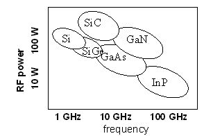
Maximum output power versus frequency
for various types of semiconductors
for various types of semiconductors
The objectives of the proposed project is to develop InAlN/(In)GaN-based devices (replacing conventional AlGaN / GaN heterostructures), and to establish the HEMT processing and characterization tools on this new material structure.
The aim is to demonstrate the feasibility of InAlN/(In)GaN-based transistors for record power capabilities.
The overall success of the project will be weighted by the following HEMT key figures of merit:
§Two-dimensional electron gas (2DEG) density ntotal > 3.7 x 1013 cm-2,
§Drain current > 3 A / mm,
§Source-drain breakdown voltage BVds> 200 V,
§Sustainable power density > 30W/mm at 10GHz, with no collapse of the drain current.
The present project aims also to strengthen the European position on commercial activities and intellectual property rights of emerged III-nitride technology. For illustration, over the last one hundred GaN-related patents, only 9 % came from Europe, while 46 % being from Japan and 24 % from US. Korea alone declared 11 % of them. With this proposal, we may be able to change this balance and possibly to get the lead in the valuable patents. Finally, we point out that InAlN/(In)GaN structure unique parameters also promise to break performance limits of teraherz devices, Bragg mirrors, microcavity LEDs, opto-modulators, and novel nano-structural devices.
Quick link:
[Welcome] [Objectives] [Consortium] [Contact] [Experts] [Publications] [People] [Private] [Legal notice]
WELCOME
TO THE EUROPEAN
PROJECT ULTRAGAN WEB SITE
TO THE EUROPEAN
PROJECT ULTRAGAN WEB SITE